


28 nm体硅工艺FPGA BRAM脉冲激光试验及翻转特性
doi: 10.11728/cjss2024.06.2024-0007 cstr: 32142.14.cjss.2024-0007
-
 薛国凤 女, 1984年6月出生于陕西省西安市, 现为中国科学院国家空间科学中心高级工程师, 主要研究方向为空间综合电子技术. E-mail: xueguofeng@nssc.ac.cn
 -
 周昌义 男, 1965年8月出生于湖北省汉川市, 现为中国科学院国家空间科学中心研究员, 博士生导师, 主要研究方向为空间综合电子技术. E-mail: zhoucy@nssc.ac.cn
作者简介:
通讯作者:
SEE Upset Characteristics of BRAM in 28 nm Bulk FPGA by Pulsed Laser Test
-
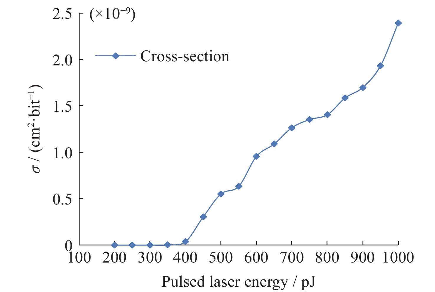
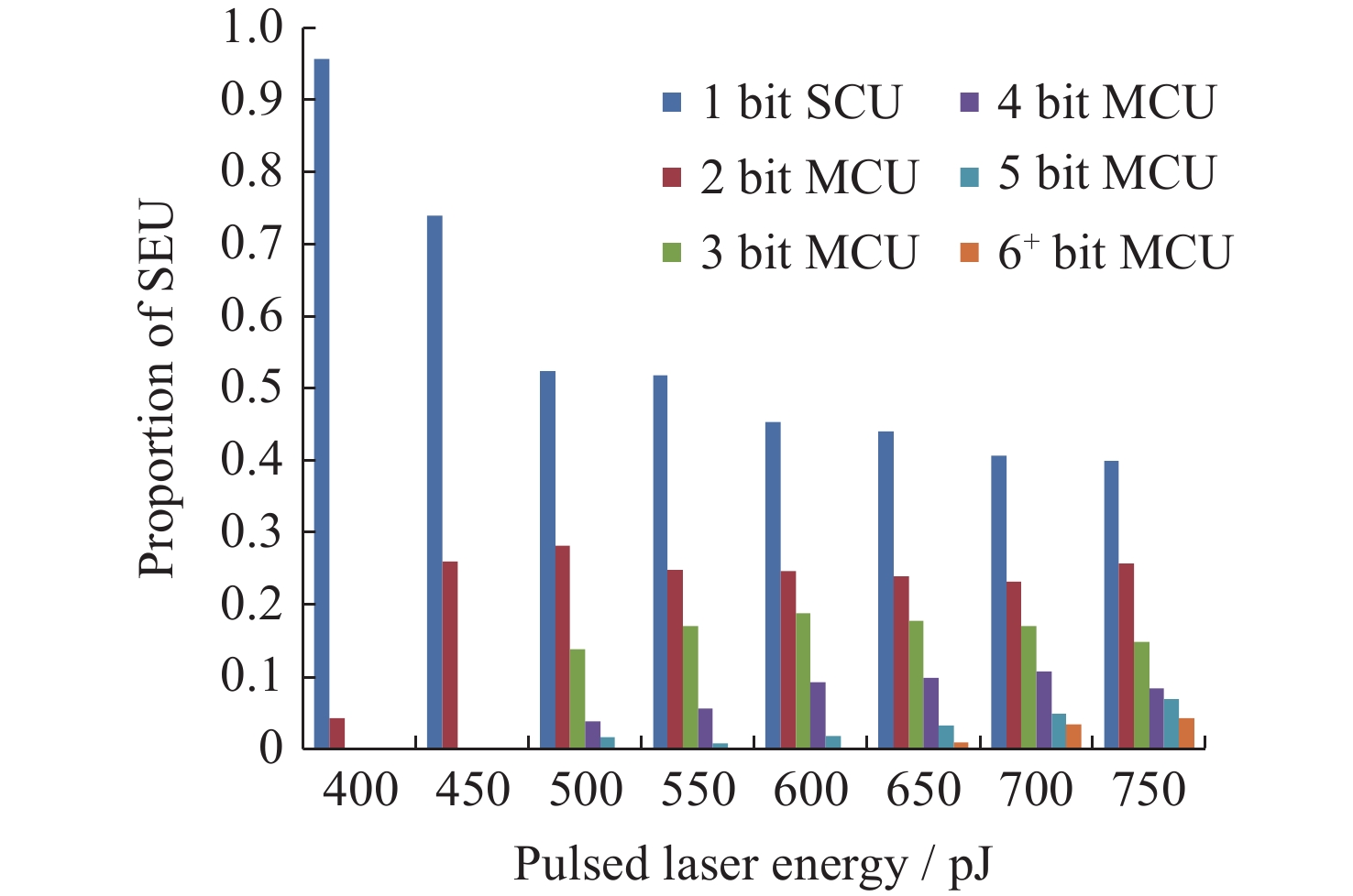
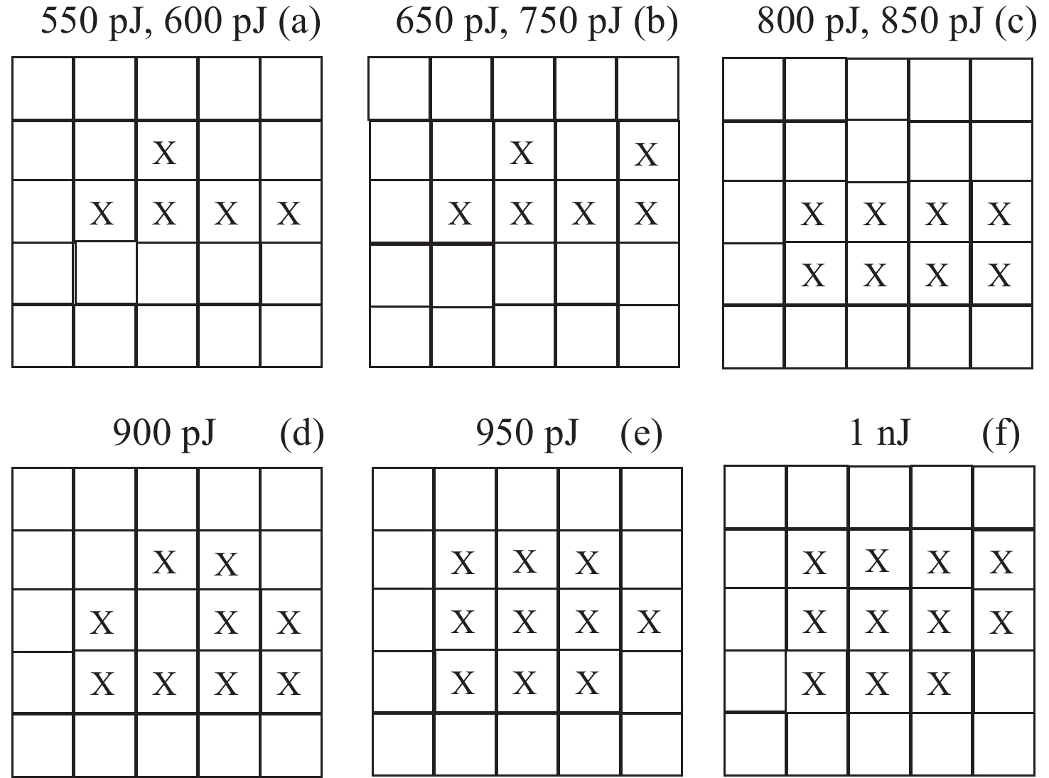
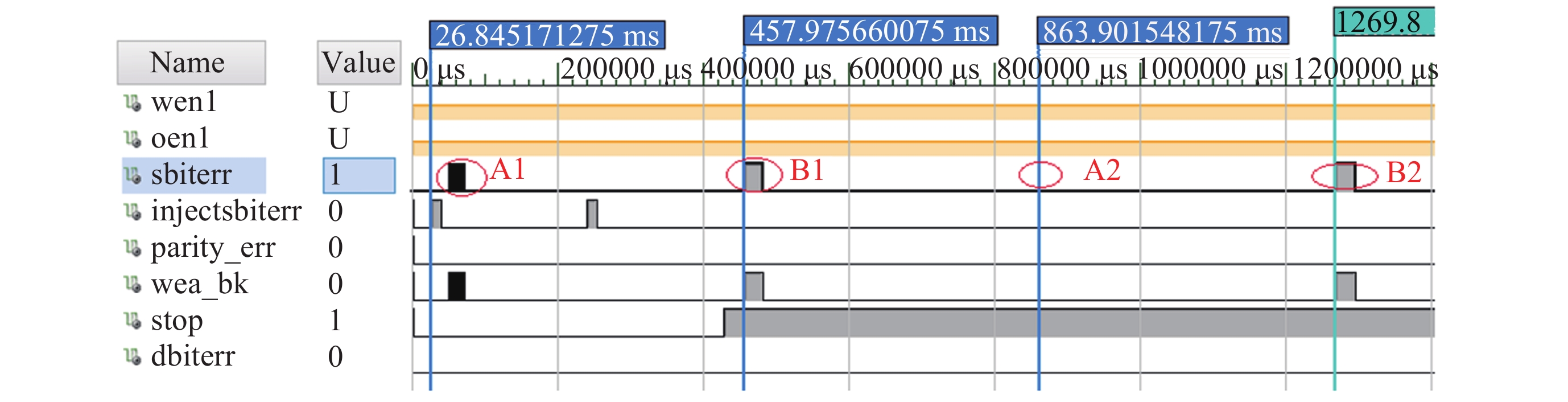
摘要: 针对SRAM型FPGA内部BRAM在轨出现翻转错误以及如何有效进行容错设计的问题, 提出了测试BRAM空间单粒子效应和多位翻转图样的方法. 多位翻转图样可以表征单次单粒子事件导致的BRAM中相邻单元的翻转特征, 进而用于分析逻辑字内是否存在多位翻转. 以XC7K410T-FFG900为研究对象, 分析其内部资源的组织结构, 采用脉冲激光试验测试BRAM的翻转特性. 通过试验测得FPGA内BRAM的翻转阈值以及在不同激光能量下的翻转截面, 并分析得到BRAM在不同能量照射下的多位翻转图样. 试验结果表明, BRAM中单个单元翻转所占比例随激光能量的增加而降低, 而多单元翻转所占比例随激光能量的增加呈上升趋势. BRAM在不同脉冲激光能量下可产生2 bit到11 bit的多单元翻转, 但通过错误注入试验验证, 该多单元翻转在单个字或者字节内并无多位翻转问题. 研究结果为提高SRAM型FPGA在航天应用中的可靠性提供了试验支持, 并依据BRAM的翻转特性给出了SRAM型FPGA在轨加固方法和建议.
-
关键词:
- 单粒子效应 /
- 脉冲激光 /
- 多单元翻转(MCU) /
- BRAM翻转图样 /
- 单粒子翻转容错
Abstract: In order to get a well-targeted Single Event Upset (SEU) mitigation for block RAM in SRAM based FPGA, a method is proposed for researching the Single Event Effect (SEE) characteristics of FPGA and get the Multiple-Cell Upset (MCU) pattern which reveal the upset mode of adjacent cells in BRAM. Pulsed laser tests were performed on 28 nm bulk Kintex-7 XC7K410T-FFG900 FPGA after analyzing the structure of configurable frame in Kintex-7 serial FPGA. The Single-Cell Upset and Multiple-Cell Upset induced by pulsed laser were observed during the test, and the cross section under different laser energy was tested. Besides, the Multiple-Cell Upset patterns of BRAM in FPGA were analyzed. The result shows that the proportion of Multi-Cell Upset climbs up with the increasing laser energy, while the proportion of Single-Cell Upset goes in the opposite way. Two to eleven bits Multiple-Cell Upset may be induced by one pulsed laser without Multiple-Bit Upset in any logical word or byte according to the error injecting test result. Some SEE mitigation methods were suggested according to the results of SEE tests to improve the reliability of SRAM based FPGA in space application.-
Key words:
- Single event effect /
- Pulsed laser /
- Multiple-Cell Upset (MCU) /
- BRAM upset pattern /
- SEU fault-tolerant
-
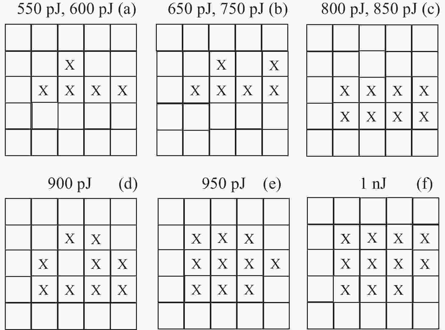
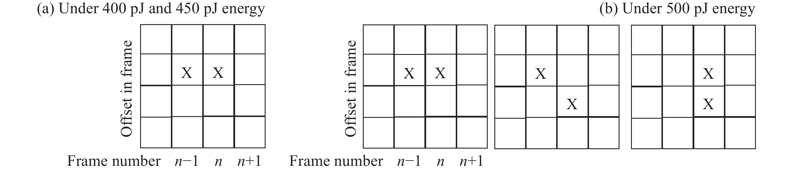
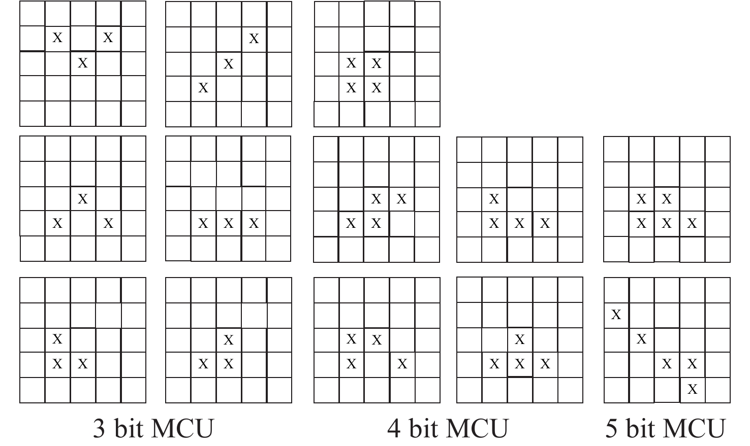
图 13 不同能量下BRAM中的最大MCU翻转图样
Figure 13. Maximum MCU upset pattern in BRAM under different energy
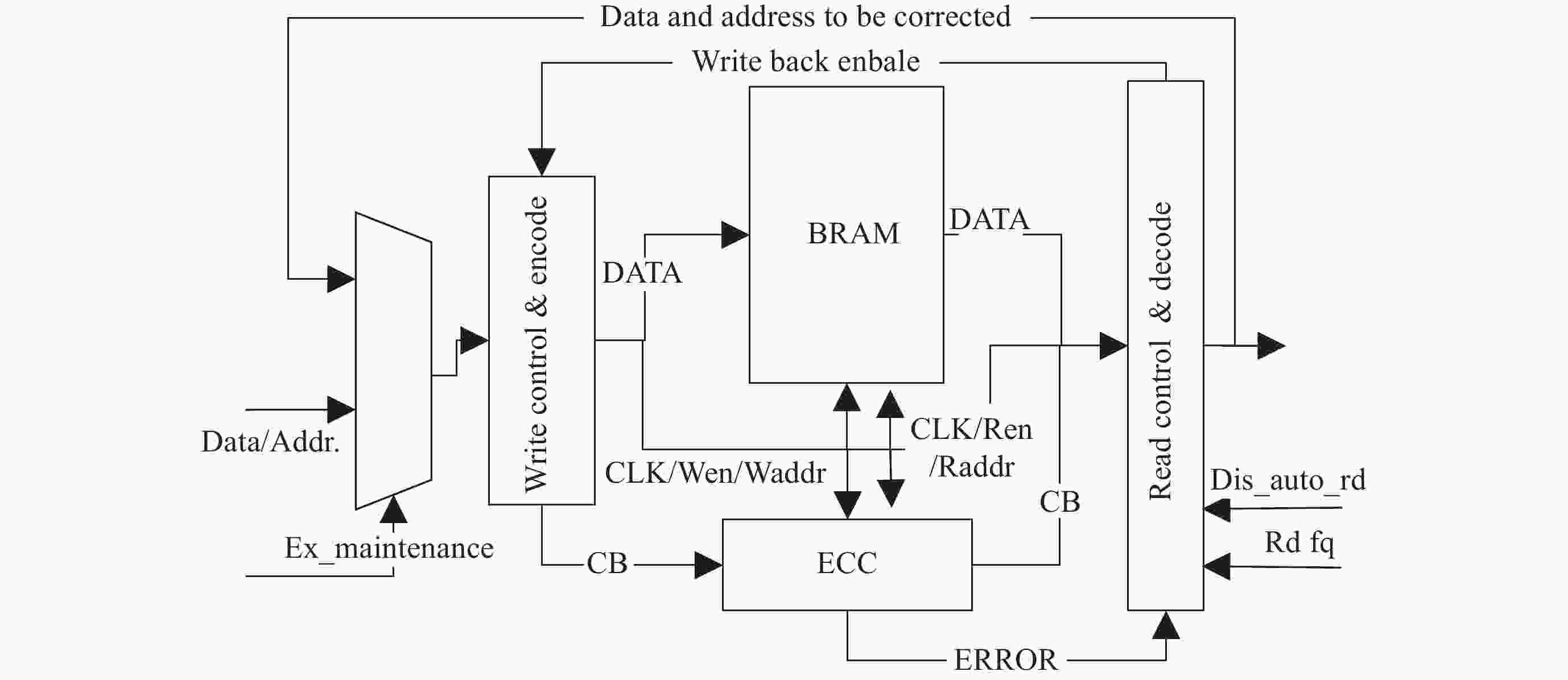
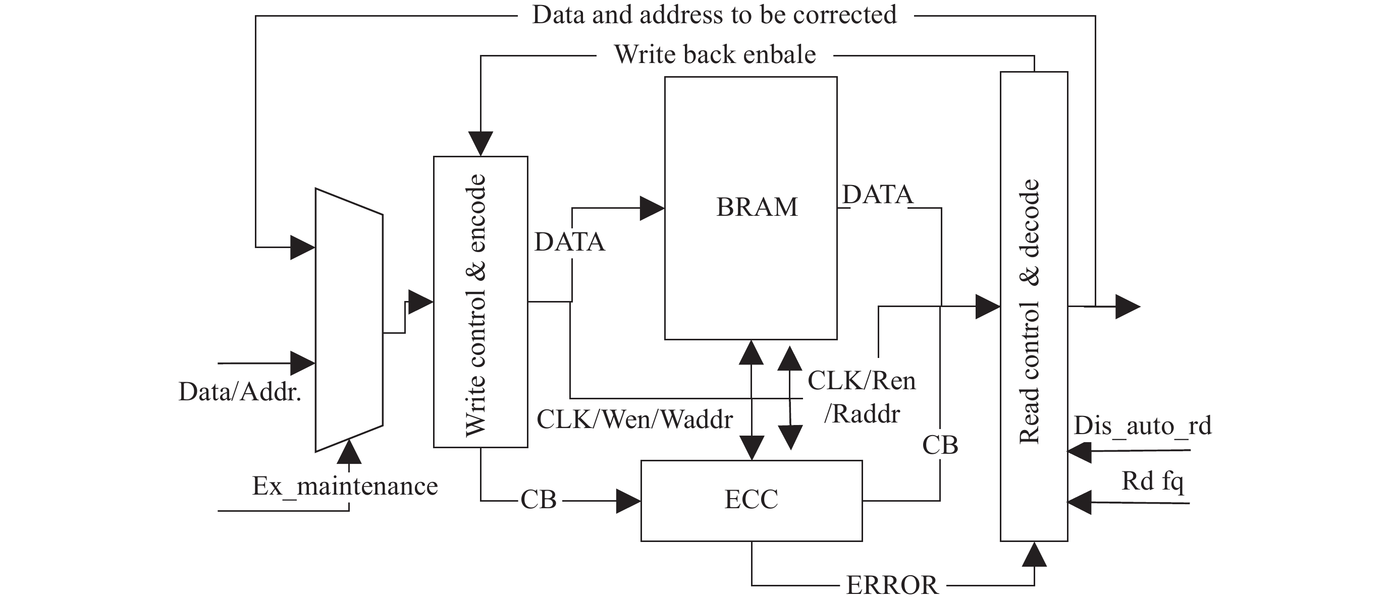
图 14 带ECC及系统维护功能的BRAM模块
Figure 14. Diagram of BRAM control logic with ECC and system maintenance
-
[1] 孙鹏跃, 刘旭辉, 毛二坤, 等. 利用分时刷新和位置约束的卫星载荷BRAM抗辐照设计方法[J]. 国防科技大学学报, 2023, 45(5): 231-236 doi: 10.11887/j.cn.202305027SUN Pengyue, LIU Xuhui, MAO Erkun, et al. BRAM anti-irradiation design method for satellite payloads using time-sharing refreshing and location constraint[J]. Journal of National University of Defense Technology, 2023, 45(5): 231-236 doi: 10.11887/j.cn.202305027 [2] TRIPPE J M, REED R A, AUSTIN R A, et al. Electron-induced single event upsets in 28 nm and 45 nm bulk SRAMs[J]. IEEE Transactions on Nuclear Science, 2015, 62(6): 2709-2716 doi: 10.1109/TNS.2015.2496967 [3] 赵元富, 王亮, 岳素格, 等. 纳米级CMOS集成电路的单粒子效应及其加固技术[J]. 电子学报, 2018, 46(10): 2511-2518 doi: 10.3969/j.issn.0372-2112.2018.10.027ZHAO Yuanfu, WANG Liang, YUE Suge, et al. Single event effect and its hardening technique in nano-scale CMOS integrated circuits[J]. Acta Electronica Sinica, 2018, 46(10): 2511-2518 doi: 10.3969/j.issn.0372-2112.2018.10.027 [4] WANG Z B, CHEN W, YAO Z B, et al. Proton-induced single-event effects on 28 nm Kintex-7 FPGA[J]. Microelectronics Reliability, 2020, 107: 113594 doi: 10.1016/j.microrel.2020.113594 [5] TONFAT J, KASTENSMIDT F L, ARTOLA L, et al. Analyzing the influence of the angles of incidence on SEU and MBU events induced by low LET heavy ions in a 28-nm SRAM-based FPGA[C]//Proceedings of the 2016 16th European Conference on Radiation and Its Effects on Components and Systems. Bremen: IEEE, 2016: 1-6. DOI: 10.1109/RADECS.2016.8093186 [6] WIRTHLIN M, LEE D, SWIFT G, et al. A method and case study on identifying physically adjacent multiple-cell upsets using 28-nm, interleaved and SECDED-protected arrays[J]. IEEE Transactions on Nuclear Science, 2014, 61(6): 3080-3087 doi: 10.1109/TNS.2014.2366913 [7] PÉREZ-CELIS A, WIRTHLIN M J. Statistical method to extract radiation-induced multiple-cell upsets in SRAM-based FPGAs[J]. IEEE Transactions on Nuclear Science, 2020, 67(1): 50-56 doi: 10.1109/TNS.2019.2955006 [8] LEE D S, WIRTHLIN M, SWIFT G, et al. Single-event characterization of the 28 nm Xilinx kintex-7 field-programmable gate array under heavy ion irradiation[C]//Proceedings of 2014 IEEE Radiation Effects Data Workshop. Paris: IEEE, 2014: 1-5. DOI: 10.1109/REDW.2014.7004595 [9] 封国强, 姜昱光, 朱翔, 等. 脉冲激光和重离子辐照FPGA产生的多位翻转效应的比较[J]. 原子能科学技术, 2014, 48(S1): 732-736FENG Guoqiang, JIANG Yuguang, ZHU Xiang, et al. Comparison of multi-bit upset in FPGA induced by pulsed laser and heavy ions[J]. Atomic Energy Science and Technology, 2014, 48(S1): 732-736 [10] XILINX. UG474(v1.8), 7 Series FPGAs Configurable Logic Block[EB/OL]. 15-16. [2016-09-27]. https://docs.xilinx.com/v/u/en-US/ug474_7Series_CLB [11] XILINX. UG470(v1.17), 7 Series FPGAs Configuration[EB/OL]. 100-100. [2023-12-05]. https://docs.xilinx.com/v/u/en-US/ug470_7Series_Config [12] 上官士鹏, 朱翔, 陈睿, 等. Flash芯片电流“尖峰”现象的脉冲激光试验[J]. 北京航空航天大学学报, 2021, 47(5): 961-966 doi: 10.13700/j.bh.1001-5965.2020.0082SHANGGUAN Shipeng, ZHU Xiang, CHEN Rui, et al. Experimental results of high current spike in Flash chip by pulsed laser[J]. Journal of Beijing University of Aeronautics and Astronautics, 2021, 47(5): 961-966 doi: 10.13700/j.bh.1001-5965.2020.0082 [13] MA Y Q, HAN J W, SHANGGUAN S P, et al. SEE characteristics of COTS devices by 1064 nm pulsed laser backside testing[C]//Proceedings of 2018 IEEE Radiation Effects Data Workshop. Waikoloa: IEEE, 2018: 1-4. DOI: 10.1109/NSREC.2018.8584271 [14] HUANG Jianguo, HAN Jianwei. Calculation of LET in SEE simulation by pulsed laser[J]. Science in China (Series G), 2005, 48 (1): 113-121 [15] 李赛, 陈睿, 韩建伟, 等. 脉冲激光诱发65nm体硅CMOS加固触发器链的单粒子翻转敏感度研究[J]. 航天器环境工程, 2021, 38(1): 55-62 doi: 10.12126/see.2021.01.009LI Sai, CHEN Rui, HAN Jianwei, et al. Sensibility of single event upset of hardened D flip-flop chain in 65 nm bulk si-licon CMOS irradiated by pulsed laser[J]. Spacecraft Environment Engineering, 2021, 38(1): 55-62 doi: 10.12126/see.2021.01.009 [16] XILINX, UG473(v1.14), 7 Series FPGAs Memory Resources[EB/OL]. 33-33. [2019-07-03]. https://docs.xilinx.com/v/u/en-US/ug473_7Series_Memory_Resources -
-

 下载:
下载:

图(15)
计量
- 文章访问数: 392
- HTML全文浏览量: 109
- PDF下载量: 31
-
被引次数:
0(来源:Crossref)
0(来源:其他)

